


Send Message
Privacy statement: Your privacy is very important to Us. Our company promises not to disclose your personal information to any external company with out your explicit permission.
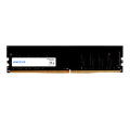
Modell: NS08GU4E8
Transport: Ocean,Land,Air,Express
Zahlungsart: L/C,T/T,D/A
Incoterm: FOB,CIF,EXW
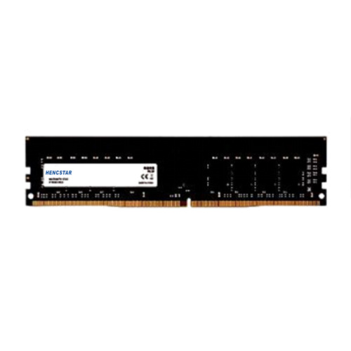
8 GB 2666 MHz 288-pin DDR4 Udimm
Revisionsgeschichte
|
Revision No. |
History |
Draft Date |
Remark |
|
1.0 |
Initial Release |
Apr. 2022 |
|
Bestellinformationstabelle
|
Model |
Density |
Speed |
Organization |
Component Composition |
|
NS08GU4E8 |
8GB |
2666MHz |
1Gx64bit |
DDR4 1Gx8 *8 |
Beschreibung
Hengstar-abgeliebter DDR4-SDRAM-DIMMS (nicht geleistete Doppeldatenrate Synchronous Dram Dual Inline-Speichermodule) sind niedrige Leistung, Hochgeschwindigkeits-Betriebsspeichermodule, die DDR4-SDRAM-Geräte verwenden. NS08gu4e8 ist ein 1G x 64-Bit-Ein-Rang 8 GB DDR4-2666 CL19 1,2V SDRAM-nicht-geklungenes DIMM-Produkt, basierend auf acht 1G x 8-Bit-FBGA-Komponenten. Die SPD ist auf JEDEC Standard Latenz DDR4-2666 Timing von 19-19-19 bei 1,2 V programmiert. Jeder 288-polige DIMM verwendet Goldkontaktfinger. Der SDRAM -abgelassene DIMM ist für die Verwendung als Hauptspeicher vorgesehen, wenn sie in Systemen wie PCs und Workstations installiert werden.
Merkmale
Stromversorgung: VDD = 1,2 V (1,14 V bis 1,26 V)
vddq = 1,2 V (1,14 V bis 1,26 V)
VPP - 2,5 V (2,375 V bis 2,75 V)
vddspd = 2,25 V bis 3,6 V
Nominale und dynamische On-Die-Staffend-Terminierung (ODT) für Daten-, Strob- und Maskensignale
Low-Power Auto Self-Aktualisierung (LPASR)
Data Bus Inversion (DBI) für den Datenbus
Die Vrefdq Generation und Kalibrierung
on-Board I2C Serienpräsenz (SPD) EEPROM
16 interne Banken; Jeweils 4 Gruppen von 4 Banken
Fixed Burst Chop (BC) von 4 und Burst Länge (BL) von 8 über den Modusregister -Set (MRS)
Ausgewählter BC4 oder BL8 im Fliege (OTF)
Databus schreiben cyclische Redundanzprüfung (CRC)
Temperatur kontrollierte Aktualisierung (TCR)
Command/Adresse (CA) Parität
Per Dram -Adressierbarkeit wird unterstützt
8 Bit vor der Abnahme
Fly-by Topologie
Command/Adresslatenz (Cal)
Befragter Kontrollbefehl und Adressbus
PCB: Höhe von 31,25 mm (1,23 ”)
Gold Randkontakte
ROHS konform und halogenfrei
Schlüsselzeitparameter
|
MT/s |
tCK |
CAS Latency |
tRCD |
tRP |
tRAS |
tRC |
CL-tRCD-tRP |
|
DDR4-2666 |
0.75 |
19 |
14.25 |
14.25 |
32 |
46.25 |
19-19-19 |
Adresstabelle
|
Configuration |
Number of |
Bank Group |
Bank |
Row Address |
Column |
Page size |
|
8GB(1Rx8) |
4 |
BG0-BG1 |
BA0-BA1 |
A0-A15 |
A0-A9 |
1 KB |
Funktionales Blockdiagramm
8 GB, 1GX64 -Modul (1Rank von x8)

absolut beste Bewertungen
Absolute maximale Gleichstrombewertungen
|
Symbol |
Parameter |
Rating |
Units |
NOTE |
|
VDD |
Voltage on VDD pin relative to VSS |
-0.3 ~ 1.5 |
V |
1,3 |
|
VDDQ |
Voltage on VDDQ pin relative to VSS |
-0.3 ~ 1.5 |
V |
1,3 |
|
VPP |
Voltage on VPP pin relative to VSS |
-0.3 ~ 3.0 |
V |
4 |
|
VIN, VOUT |
Voltage on any pin except VREFCA relative to VSS |
-0.3 ~ 1.5 |
V |
1,3,5 |
|
TSTG |
Storage Temperature |
-55 to +100 |
°C |
1,2 |
DRAM -Komponente Betriebstemperaturbereich
|
Symbol |
Parameter |
Rating |
Units |
Notes |
|
TOPER |
Normal Operating Temperature Range |
0 to 85 |
°C |
1,2 |
|
Extended Temperature Range |
85 to 95 |
°C |
1,3 |
AC & DC -Betriebsbedingungen
Empfohlene DC -Betriebsbedingungen
|
Symbol |
Parameter |
Rating |
Unit |
NOTE |
||
|
Min. |
Typ. |
Max. |
||||
|
VDD |
Supply Voltage |
1.14 |
1.2 |
1.26 |
V |
1,2,3 |
|
VDDQ |
Supply Voltage for Output |
1.14 |
1.2 |
1.26 |
V |
|
|
VPP |
Supply Voltage for DRAM Activating |
2.375 |
2.5 |
2.75 |
V |
3 |
Modulabmessungen
Vorderansicht

Rückansicht

Produktgruppe : Industrielles Smart -Modulzubehör


Privacy statement: Your privacy is very important to Us. Our company promises not to disclose your personal information to any external company with out your explicit permission.
Fill in more information so that we can get in touch with you faster
Privacy statement: Your privacy is very important to Us. Our company promises not to disclose your personal information to any external company with out your explicit permission.